In the realm of digital electronics, AND logic gate are ubiquitous and vital components. These gates are the building blocks of complex computational logic, enabling the processing of binary data essential to computer systems and various electronic devices. This comprehensive guide delves into the intricacies of AND logic gates, providing a detailed look at their circuit diagrams, truth tables, symbols, and practical applications in integrated circuits (ICs).
Whether you’re a student, an enthusiast, or a professional in the field, understanding the function and implementation of AND gates is crucial for mastering digital electronics. We will explore the schematic representation, decode the truth tables, identify the symbols, and examine the inner workings of AND gate ICs. By the end of this exploration, you will have a complete understanding of AND logic gates and their role in the digital world. Let’s expand on each aspect of AND logic gates for a more comprehensive understanding.
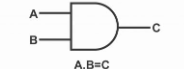
AND Logic Gate Circuit Diagram
The circuit diagram of an AND logic gate is quite simple, consisting of a standardized symbol. This symbol is universally recognized in digital electronics and is often represented by a flat edge on one side (where inputs are entered) and a curved edge on the other side (from where the output is taken). The standard AND gate symbol has two input lines coming into the flat edge and one output line coming from the curved side. In a circuit diagram, the connections to other components are shown coming in and out of this symbol.
AND Logic Gate Truth Table
The truth table for an AND gate is a tabular representation of all possible input combinations and their corresponding outputs. For a two-input AND gate, the truth table has four possible input combinations:
| Input A | Input B | Output (A AND B) |
|---|---|---|
| 0 | 0 | 0 |
| 0 | 1 | 0 |
| 1 | 0 | 0 |
| 1 | 1 | 1 |
This table clearly shows that the output is only high (1) when both Input A and Input B are high (1).
AND Logic Gate Symbol
The symbol used in schematic diagrams to represent an AND gate is designed to be distinct and easily recognizable. It consists of a shape that looks somewhat like a stretched ‘D’ with two lines entering from the left, which are the inputs, and one line exiting to the right, which is the output. The inputs are labeled, typically as A and B, and the output as C or Q or Y.
AND Logic Gate Circuit
A practical AND gate circuit can be constructed using various components. In semiconductor technology, transistors are the most common. For instance, two transistors can be connected in series with their collectors connected to the power supply, and their emitters grounded through a resistor. Both transistors must be conducting for the output at the junction between the transistors and the resistor to be high, thus implementing the AND logic.
AND Logic Gate Diagram
A diagram of an AND gate can show a more detailed internal view, often including the transistors, diodes, or resistors that make up the gate. The diagram would illustrate how the components are connected to achieve the desired logic behavior.
AND Logic Gate IC
Integrated circuits (ICs) for AND gates, such as the 7408, are small chips that can contain multiple individual AND gates. The IC will have a pinout diagram showing where the inputs and outputs for each gate are located on the chip. These ICs are used extensively in digital electronics for compact and reliable logic operations.
AND Logic Gate Description
An AND gate can be described as a basic digital logic gate that implements logical conjunction – it outputs true only if all the inputs are true. This behavior is based on the concept of Boolean algebra, and AND gates are the electronic embodiment of the logical “and” function.
AND Logic Gate Sign
The sign or symbol for an AND gate is the D-shaped graphic used in logic diagrams. It is part of a family of symbols used to represent different logic operations in electronics. Being able to recognize this sign is essential for anyone working with or learning about digital circuits.
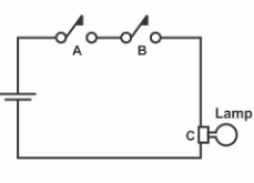
AND Logic Gate Switch
An educational way to demonstrate an AND gate is using two mechanical switches connected in series. If both switches are closed (representing a logical ‘1’), current flows through the circuit and can, for instance, light up a bulb or activate a buzzer.
AND Logic Gate Transistor
When using transistors to build an AND gate, the transistors must be arranged so that the output is high only when both transistors are allowing current to pass through. This is typically achieved by connecting the transistors in series, where the output is taken from the point between them.
AND logic gates are more than just a fundamental concept in digital electronics; they are the linchpins of logical decision-making in electronic devices. Through circuit diagrams, we have visualized their structure, while truth tables have elucidated their logical operations. Symbols have given us a language to represent these gates in schematics, and ICs have shown us how they are packaged into the functional units of modern technology. From simple educational models using switches to complex circuits driving the latest computing technology, AND gates demonstrate the elegance of digital logic. With this knowledge, one can appreciate the simplicity and power of digital logic that starts with these basic gates and scales up to the most advanced microprocessors driving today’s digital revolution. This guide has aimed to equip you with a thorough understanding of AND logic gates, an essential step on the journey to mastering digital electronics.
Frequently Asked Questions
What is the logic of an AND gate?
The logic of an AND gate dictates that it outputs a high signal (1) only when all its inputs are high. If any of the inputs are low (0), the output is low. The AND gate is a basic digital logic gate that implements logical conjunction – following the logical operation “and.”
What does ‘and’ do in logic gates?
The ‘and’ in logic gates refers to the logical AND operation, which outputs a true (1) signal only when all the inputs are true. If any of the inputs are false (0), the output is false. In essence, the ‘and’ operation in logic gates is a gatekeeping function that allows a signal to pass only when all conditions are met.
What is the purpose of an AND gate?
The purpose of an AND gate is to provide a true output only when all the conditions represented by the inputs are true. It serves as a fundamental building block in digital circuits and is used for decision-making operations, where multiple factors must be true for an action to be taken or a signal to be sent.
What is the function of a logic gate ‘and’?
The function of a logic gate ‘and’, or AND gate, is to perform the AND operation, meaning it outputs a high signal only when all its inputs are high. This function is crucial in computational logic for combining multiple boolean conditions. The AND gate is instrumental in creating complex logic circuits and is used extensively in computer operations and digital systems.