
Before understanding the 8086 Pinout Diagram, we will understand what is microprocessor. A microprocessor is a computer processor. The microprocessor contains the arithmetic, logic, and control circuit required to perform the function of the computer’s central processing unit. The microprocessor is an electronic device. Microprocessors also denote something very little like a very small processor or microprocessor. The microprocessor is fundamentally the brain of the computer. All the functions of the processor are included on a single chip.
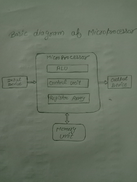
This is a circuit diagram of the microprocessor.
Microcontroller
A microcontroller is a compact integrated circuit designed for specific operations in an embedded system. The microcontroller includes a processor, memory, and input and output peripherals on a single chip. The microcontroller is used to automatically control products and devices such as automobile engine control systems.
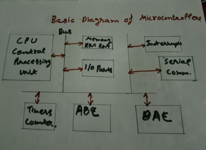
This is a diagram of the microcontroller.
8086 processor
The 8086 microprocessor is an enhanced version of the 8085 microprocessor. It was designed by INTEL in 1976. The 8086 microprocessor has 20 address lines and 16 data lines. It is 16 bits microprocessor. Microprocessor consists of a powerful instruction set, which provides operations such as division and multiple easily.
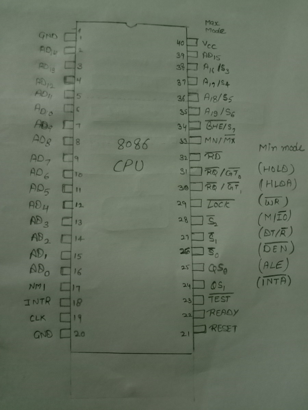
8086 Pinout Diagram microprocessor.
Power supply and frequency signals
It uses a 5v Dc supply at VCC pin 40 and ground at VSS pins 1 and 20 for its operation.
Clock signal
The clock signal is provided through Pin-19. Clock signal supply timing to the processor for operations. The frequency of the clock signal is different for different versions such as 5MHz, 8MHz, and 10MHz.
Address and data bus
AD0-AD15. These are 16 addresses and data buses. AD0-AD7 carries low-order byte data and AD8-AD15 higher-order byte data.
Address and status of bus
From A16-A19 and S3-S6 These are the 4 address and status buses. In the first clock cycle, it carries a 4-bit address, and later it carries status signals.
S7and BHE
BHE stands for Bus High Enable. BHE is available at pin 34 and used to indicate the transfer of data using data bus D8-d15.
Read
Read is to hand at pin 32 and is used to read signal for operations.
Ready
Ready is to hand at pin 22. Ready is an acknowledgment signal from input\output devices that data is transferred. This is an active high signal.
Reset
It is to hand at pin 21 and is used to restart the execution. It causes the processor to immediately terminate its present activity.
INTR
The INTR is available at pin 18. The INTR is an interrupt request signal, which is sampled through the last clock cycle of each instruction to determine if the processor considered this as an interrupt.
NMI
NMI stands for non-maskable interrupt and is to hand at pin 17. The NMI is an edge-triggered input, which causes an interrupt request to the microprocessor.
INTA
The INTA is an interrupt acknowledgment signal and id available at pin 24. When the microprocessor receives this signal, it acknowledges the interrupt.
ALE
ALE stands for address enable latch and is to hand at pin 25. When begins any operation, the positive pulse gives rise to each time the processor.
DEN
It stands for Data Enable and is available at pin 26. DEN is used to enable Transreceiver 8286.
DT\R
It stands for Data transmit\ receive signal and is available at pin 27. DT\R decides the direction of data flow during the transceiver.
HLDA
The HLDA stands for Hold Acknowledgement signal and is available at pin 30. This signal acknowledges the Hold signal.
HOLD
The signal indicates to the processor that external devices are requesting to access the address\data buses. The pin of hold is 31.
S0, S1, S2
These are the status signals that provide the status of the operation, which is used by the Bus Controller 8288 to give memory and input\output control signals.
LOCK
When the lock signal is active, it indicates to the other processor not to ask the CPU to leave the system bus.
RQ\RT1 and RQ\GT0
The RQ\RT1 and RQ\GT0 are the Requests \ Grant signals used by the other processor requesting the CPU to release the system bus.
8051 Microcontroller
The 8051 microcontroller is outlined by INTEL in 1981. The 8051 microcontroller is an 8-bit microcontroller. It is made with 40 pins. The ROM storage is 4kb and the RAM storage is 128 bytes of this processor.

The 8051 processor is used for home applications such as home security systems, video games, and music instruments.
8051 processor pin diagram
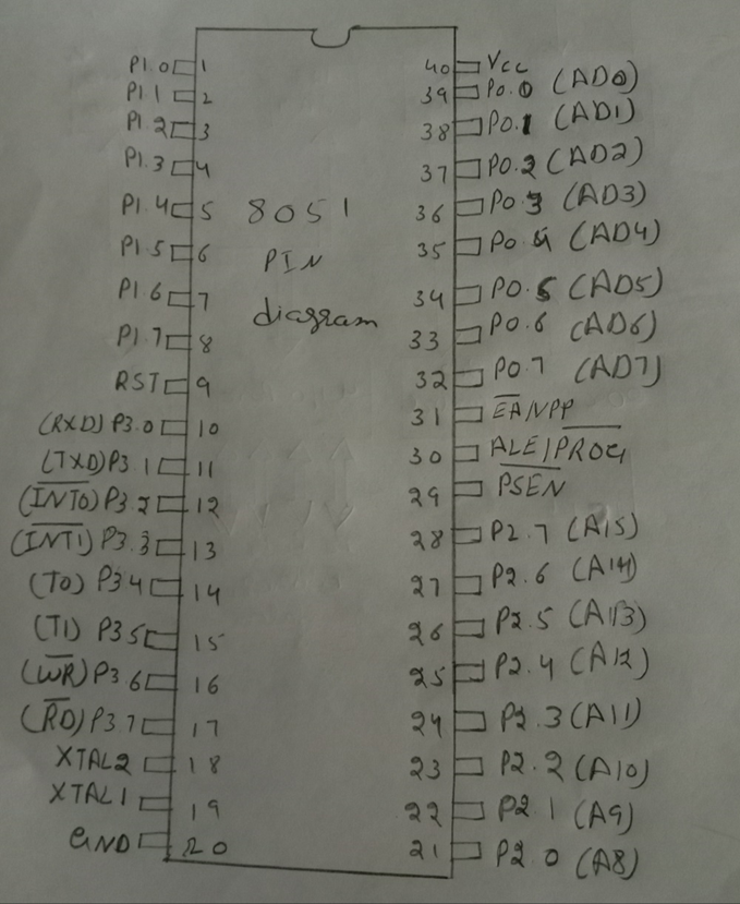
Pin 1 to Pin 8 (port 1)
Pin 1 to Pin 8 is assigned to port 1 for simple input and output operations. Pin 1 to Pin 8 can be configured as input or output pins depending on the logic control.
PIN RESET
The reset pin is an active- high, input pin. It is mostly used for resetting the processor.
Pin 10 to Pin 17(port3)
Pin 10 to Pin 17 are port 3 pins which are also referred to as P3.0 to P3.7. These pins are bidirectional pins.
RXD AND TXD
The RXD pins are serial data receive pins and the TXD pins are serial data transmit pins.
INT0 AND INT1
The int0 and int1 (12th and 13th) pins are for external hardware interrupt0 and interrupt1.
T0 AND T1
T0 and T1 Pin are for Timer 0 and Timer 1 external input.
WR AND RD
The 16th pin is for external memory write and 17th pin is for external memory read.
PIN 18 AND PIN 19 (XTAL2XTAL1)
These pins are connected to an external oscillator which is generally a quart crystal oscillator.
Pin 20 (GND)
This pin is connected to the ground. The ground has to be provided with a 0v power supply.
Pin 21 to Pin 28 (port 2)
These pins are bidirectional. When additional external memory is interfaced with 8051 microcontrollers.
Pin 29(PSEN)
PSEN stands for program store Enable. It is used to read external memory. This pin output, an active low pin.
Pin 30(ALE\PROG)
ALE stands for Address Latch Enable. It is input, active- high pin. ALE is used to distinguish between memory chips.
Pin 31(EA\VPP)
EA stands for external access input. It is used to enable\ disable external memory interfacing.
Pin 32 to Pin 39 (port 0)
Pin 32 to Pin 39 are port 0 pins also referred to as P0.0 to P0.7. They are bidirectional input\output pins.
Pin 40(VCC)
This pin provides power supply voltages that are Volts to the circuit.
Also Read raspberry pi pico pinout diagram